

AMD Blueprint for Zen 6 Unveils Multi-Generational Low-Power CPU Core Design
Linux kernel patches reveal a three-tier silicon strategy built from five generations of Zen microarchitecture.
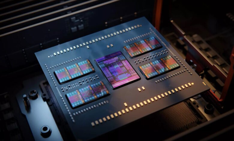
Operating systems rely on structural maps known as CPU topology to correctly distribute tasks across silicon, but recent patches submitted to the Linux kernel show AMD preparing for an unconventional hardware setup in its upcoming Zen 6 processor family. The code modifications reveal that AMD is introducing a dedicated class of low-power cores designed so differently from existing architectures that Linux currently flags them as unknown hardware until explicitly patched.
Rather than constraining these low-power cores to a fixed hardware performance ceiling—traditionally assigned via the static CPPC_HIGHEST_PERF_PERFORMANCE parameter—the updated software path enables dynamic scaling on supported AMD and Hygon processors through the amd_get_highest_perf() interface. This adjustment relies on Collaborative Processor Performance Control (CPPC), an ACPI standard that allows the operating system kernel to continuously negotiate clock frequencies and power limits with onboard microcontrollers based on real-time task demands. Complete details on kernel hardware management interfaces are maintained in the Linux Kernel Archives.
A hardware component analysis highlighted by processor researcher InstLatX64 reveals that these low-power cores are assembled from building blocks spanning five distinct generations of AMD silicon. The reported design fuses a Zen 6 instruction set architecture (ISA) with a Zen 5 execution microarchitecture, a Zen 4 floating-point unit (FPU), a Zen 3 L2 cache, and a Zen 2 L3 cache.
This composite approach allows AMD to bypass the immense development cost and physical engineering timeline required to design an ultra-low-power architecture from scratch. In chip design, the Instruction Set Architecture defines the vocabulary of commands software can send to the processor, while the microarchitecture represents the physical circuits that execute those commands. By pairing modern front-end instruction decoders with older, physically smaller floating-point units—which process math-heavy vector operations—and compact legacy cache structures, AMD retains modern software compatibility while sharply reducing physical die area and baseline power draw.
The integration of these units creates a three-tier compute topology. Standard Performance cores target high-frequency, single-threaded processing, while compact Efficiency cores (AMD’s compact “C” variants) manage high-density multithreaded operations. The new low-power cores form a third layer dedicated to ultra-light background processes. While this operational focus targets the same power-saving goals as Intel’s low-power efficiency cores, AMD achieves it through modular IP reuse rather than a single dedicated microarchitecture.
The operational benefits are most pronounced in mobile form factors like ultrabooks and portable gaming handhelds. Offloading ambient system tasks to dedicated cores capable of running within an envelope of just a few watts enables primary compute clusters to power down completely. However, the real-world impact will depend heavily on thread scheduling, as software drivers must accurately route background workloads without introducing execution stalls on the legacy cache structures.
These architectural details surface as AMD prepares its Zen 6 server chips for deployment, with desktop variants slated to follow later this year. This hardware transition comes amid headwinds in the broader PC market, where shipment contraction and rising memory prices—driven by high demand for AI hardware—continue to raise total platform costs. Because mobile processors are permanently integrated into system boards, requiring full device replacements for upgrades, adoption rates for this multi-generational core architecture will hinge on whether its efficiency gains deliver tangible battery life improvements to end users.