
Nvidia, Cisco Unveil USFP Optical Standard for AI Data Centers
The 400G per-lane pluggable interface targets 12.8Tb/s total bandwidth to eliminate network bottlenecks in GPU clusters.
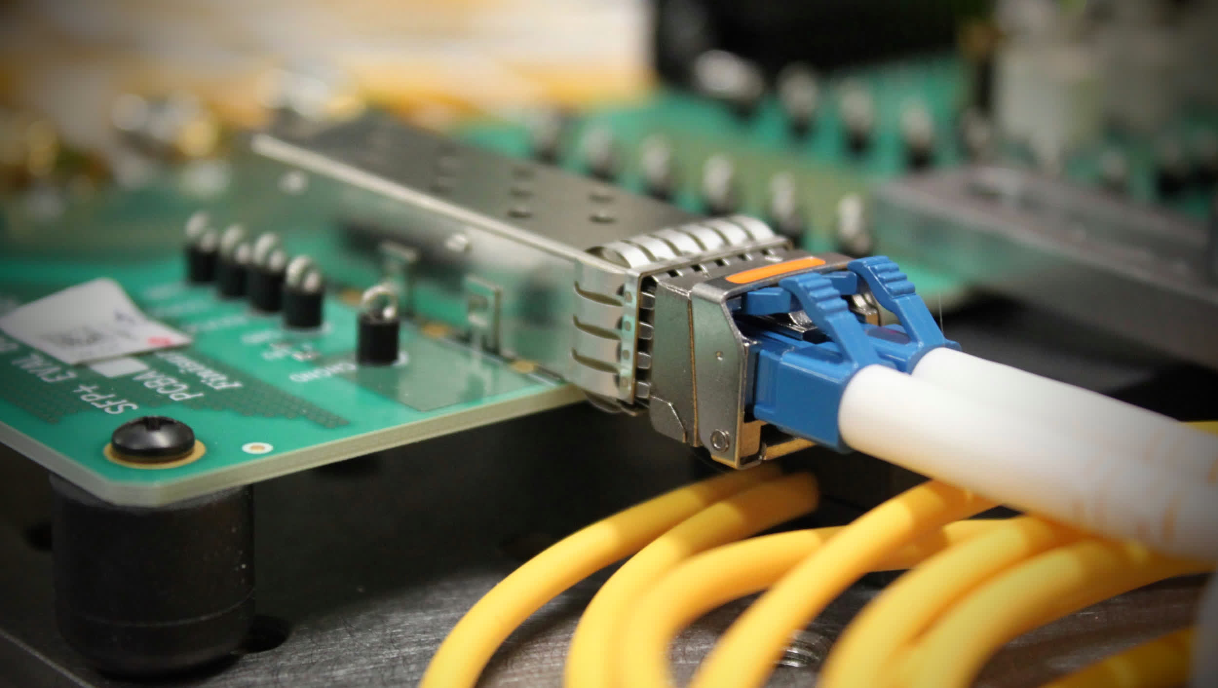
Nvidia and Cisco have jointly developed the Ultra-Dense Small Form Factor Pluggable (USFP), a new optical transceiver interface engineered to push data center interconnect speeds to 400 gigabits per second per lane. The specification targets a long-term ceiling of 12.8 terabits per second, positioning it as the fastest pluggable optical networking standard designed specifically for artificial intelligence infrastructure.
The immediate bottleneck in AI data centers is no longer raw compute power but the ability to move massive datasets between thousands of GPUs without latency penalties. Current industry deployments rely heavily on 800G optical modules using 100G or 200G per-lane signaling. By doubling the per-lane speed to 400G, USFP quadruples total bandwidth capacity compared to 200G-per-lane interfaces while delivering a 1.3x improvement in power efficiency. That efficiency gain addresses one of the most pressing operational constraints in hyperscale facilities, where power delivery and thermal management dictate how densely GPU clusters can be packed.
Initial USFP-based transceivers will ship with 16 full-duplex lanes housed in an octal small form factor footprint. These modules are designed to plug directly into both traditional network switches and SuperNICs. Nvidia’s SuperNIC architecture, utilized across its Quantum and Spectrum-X platforms, accelerates data movement directly between GPUs using RDMA over Converged Ethernet (RoCE). RoCE bypasses the host CPU entirely, allowing remote direct memory access over standard Ethernet fabrics—a requirement for synchronizing the massive tensor parallelism workloads used to train large language models.


The physical design of the USFP module introduces a two-step insertion mechanism aimed at preserving signal integrity at extreme frequencies and reducing mechanical wear on contacts during hot-swapping. Because high-speed optical modules generate significant heat, the interface supports up to 100 watts of power dissipation without requiring a dedicated internal cooling circuit within the transceiver itself, relying instead on the host chassis airflow.
Scaling beyond the initial 16-lane configuration, the roadmap calls for 32 or more lanes. This expansion would allow network architects to connect additional 1.6Tb/s endpoints without introducing extra switching tiers. Flattening the network topology reduces hop count, which directly decreases tail latency—the unpredictable delays that stall synchronized AI training jobs.
To prevent supply chain bottlenecks, Nvidia and Cisco have already enlisted TE Connectivity and Amphenol to manufacture the cages, connectors, and supporting hardware required for the USFP ecosystem. Opening component manufacturing to established third-party interconnect vendors mirrors the strategy used to scale previous standards like QSFP-DD and OSFP, ensuring hyperscalers can source compatible hardware from multiple suppliers.
Pluggable optics like USFP represent one vector in a broader industry transition toward advanced silicon photonics. Hyperscalers are simultaneously evaluating co-packaged optics, where optical engines are mounted directly adjacent to switch ASICs to minimize electrical trace losses, and near-packaged architectures. While co-packaged optics offer theoretical density advantages, they complicate field maintenance because a single failed optical link can require replacing an entire switch board. USFP maintains the serviceability of traditional pluggable modules while pushing their performance closer to the physical limits of copper-to-optical conversion.
TE Connectivity and Amphenol are currently ramping production of the physical interface components, with the first 16-lane USFP transceivers expected to enter validation testing inside next-generation AI fabric deployments.