

CXMT Launches G5 DRAM as China Pushes Past Chip Restrictions
China’s CXMT brings 11.95nm memory technology into mass production
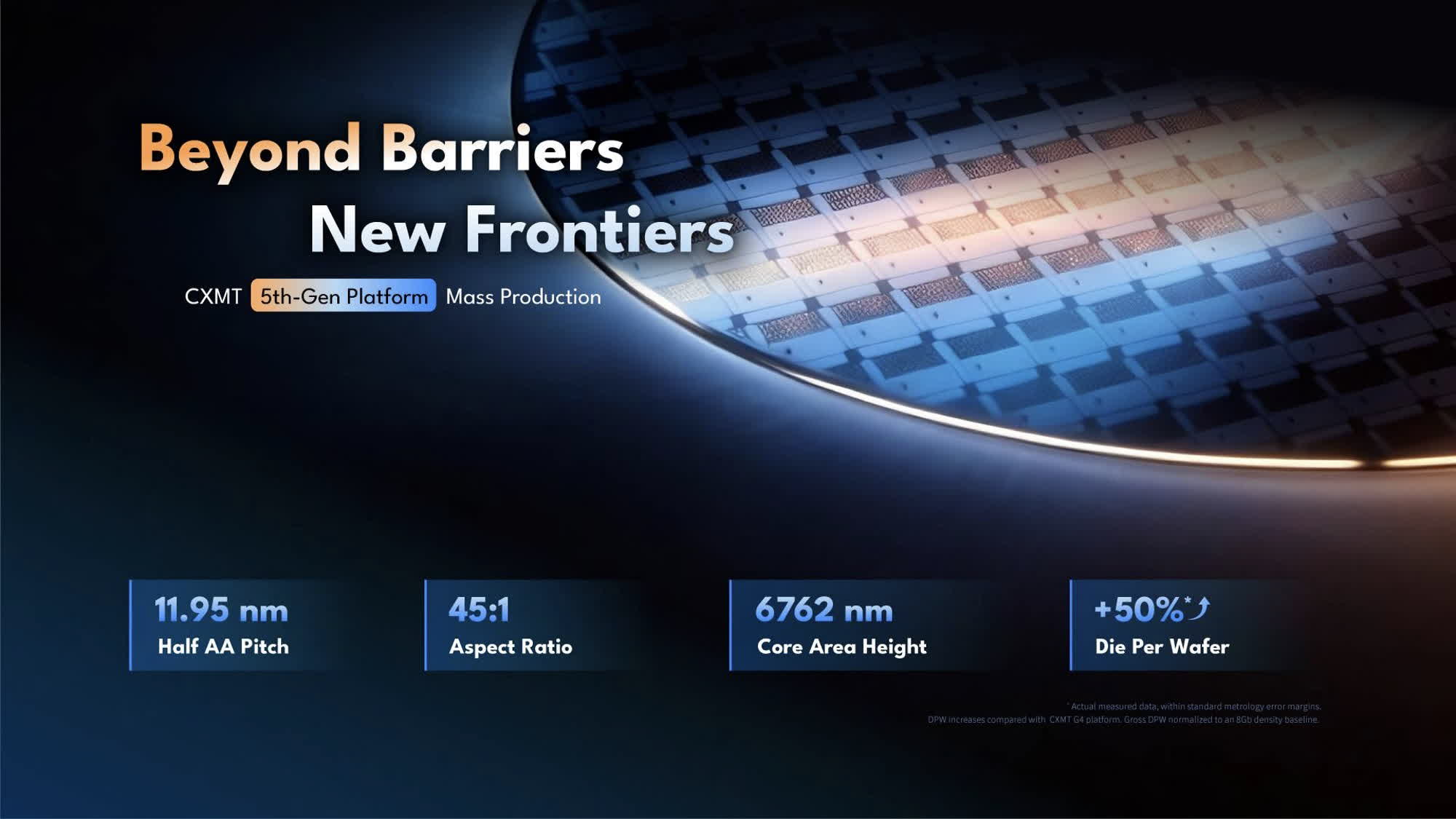
ChangXin Memory Technologies (CXMT) is initially using its fifth-generation dynamic random-access memory (DRAM) technology to mass-produce two low-power double data rate 5X (LPDDR5X) products. Designed for smartphones, laptops, and other portable computing devices, the chips offer a capacity of 24 gigabits (Gb) per die, a 50% increase in density over the manufacturer’s previous-generation offerings.
The Hefei-based chipmaker announced the commercial rollout of its new “G5 Platform” at the 2026 World Manufacturing Convention. CXMT stated that the platform achieves manufacturing capabilities rivaling the most advanced, mass-produced nodes currently offered by global market leaders such as Samsung Electronics, SK Hynix, and Micron Technology.
The new technology raises die-per-wafer density by 50% compared with CXMT’s previous generation of DRAM. The company claims the improvement will significantly enhance power efficiency. CXMT has also begun preparing for further growth, expanding manufacturing capacity and planning to scale up wafer output to unprecedented levels to meet anticipated domestic and international demand.


CXMT’s G5 Platform uses self-aligned quadruple patterning (SAQP) technology to achieve an active-area half-pitch of 11.95nm for its memory arrays. The multi-patterning approach allows the company to manufacture high-density memory chips with older Deep Ultraviolet (DUV) lithography equipment.
That engineering approach has become important as Chinese firms lack access to state-of-the-art Extreme Ultraviolet (EUV) lithography systems from Dutch manufacturer ASML. Since 2022, the U.S. Department of Commerce has imposed sweeping export controls intended to limit Chinese manufacturers’ access to equipment capable of producing DRAM chips at or below the 18-nanometer (nm) half-pitch threshold.
CXMT stated that SAQP is only one of several engineering breakthroughs integrated into the G5 Platform. The company redesigned its chip architecture through novel material integration, achieving an array capacitor aspect ratio of 45:1. It also implemented a DRAM-optimized high-k metal gate (HKMG) process that reduced the core cell array height to exactly 6,762nm.
To shorten the development cycle, CXMT used “digital twin” technology. The process involved creating virtual models of the hardware for design, tape-out, manufacturing, and yield management. CXMT stated that the digital modeling approach significantly reduced the time required to establish complex DRAM process models.
Founded in 2016 with backing from Chinese state-affiliated entities, including the National Integrated Circuit Industry Investment Fund, known as the “Big Fund,” CXMT has emerged as China’s champion in the DRAM market. The global DRAM sector has historically been highly consolidated, with Samsung, SK Hynix, and Micron collectively controlling roughly 90% of global market share.
The commercial rollout comes amid intensifying geopolitical competition between Washington and Beijing over access to advanced semiconductor technology. It also arrives during a period of highly volatile valuations in the global memory sector. Western companies face persistent regulatory scrutiny regarding Chinese suppliers, similar to the political pressure that blocked Apple Inc. from finalizing a supply agreement with Chinese flash-memory manufacturer Yangtze Memory Technologies (YMTC) in 2022.
Speculation remains that Apple and other major global electronics brands could eventually look to integrate CXMT’s chips into their consumer products.